银管(Ag)

高纯银管具备卓越的导电率与热导性,表面光洁、结构致密,适用于电子器件、电极引线、真空系统及科研装置。提供多种规格与纯度,可定制毛细管及抛光表面,满足高端制造与实验需求。

描述

银管(Ag Tube)

产品简介

银管(Ag Tube)是一种由高纯银制成的贵金属管材,具有优异的导电性、导热性和抗氧化性能。银是所有金属中电导率和热导率最高的材料之一,因此银管在高精度电子器件、真空系统、电极组件和光电应用中具有重要作用。其优良的化学稳定性与延展性,使其成为科研和高端制造领域不可或缺的功能材料。

产品详情

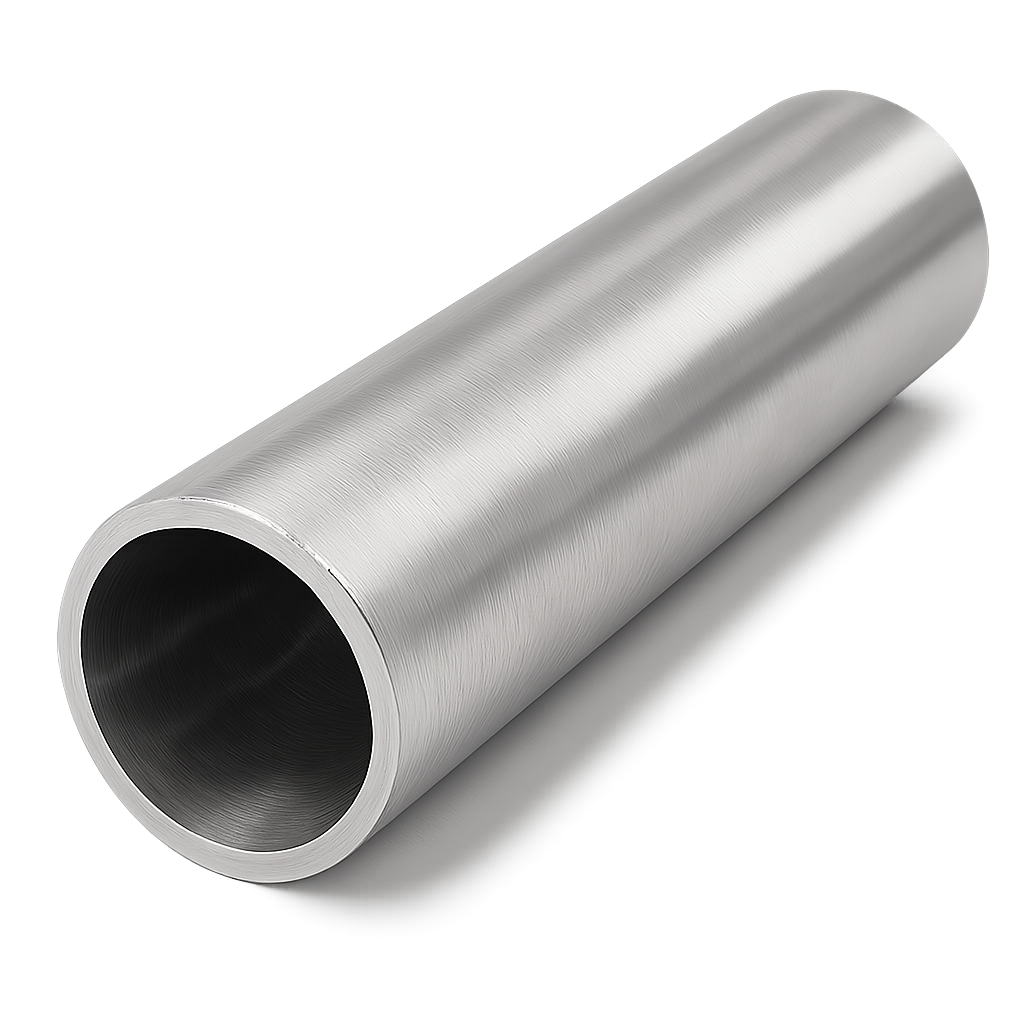
苏州科跃材料科技有限公司生产的银管选用高纯银(纯度≥99.9%)作为原料,经真空熔炼、挤压与冷拉成型工艺制成,结构致密,表面光滑,无裂纹和夹杂物。
可提供以下典型规格:

  • 纯度等级:99.9%、99.99%、99.999%

  • 外径范围:0.5 – 60 mm

  • 壁厚范围:0.1 – 5 mm

  • 长度:≤1000 mm(可按需定制)

  • 表面处理:光亮、抛光、退火状态

采用真空退火与精密整形技术,银管具备优异的延展性,可进行精密弯管、焊接或微结构加工。对于高频与真空系统应用,可提供低杂质、低孔隙版本以提升电导与真空兼容性。

应用领域

银管广泛应用于高科技领域的电气与热管理系统:

  • 电子与半导体工业:用于高导电电极、引线管、互连管及传感器封装。

  • 真空与光电系统:在真空腔体、光电探测装置中作为导流与连接元件。

  • 热交换与导热组件:作为高效导热通道,用于温控装置或散热系统。

  • 化学与分析仪器:用于惰性反应环境下的气体输送与检测管。

  • 医疗与实验设备:应用于生物传感器、电极及微流控系统。

技术参数

参数 典型值 / 范围 说明
纯度 99.9% – 99.999% 纯度越高,导电性与稳定性越好
外径 0.5 – 60 mm 支持定制
壁厚 0.1 – 5 mm 适配不同压力和强度需求
密度 10.49 g/cm³ 保证高导热与结构稳定性
电导率 62 × 10⁶ S/m 金属中最高之一
熔点 961.8 °C 适合高温导电环境
工艺 真空熔炼 + 冷拉 + 退火 保持优异纯度与延展性

常见问题(FAQ)

问题 答案
银管是否易氧化? 银表面易生成一层薄硫化膜,但不影响导电性能。可选防氧化处理。
可否用于高频电极? 可以,银管具有极低电阻损耗,非常适合高频或微波电路应用。
可提供多长尺寸? 单根最长可达 1 米,可按客户要求定制切割。
是否支持焊接? 可以进行真空钎焊或惰性气氛焊接。
能否制作毛细管? 是的,最小内径可达 0.1 mm,用于微流体或探针系统。
可否用于真空系统? 可以,高纯银管在真空中化学稳定,不释放气体。
银管的热导性能如何? 银的热导率约为 429 W/m·K,为金属中最高之一。
可提供检测报告吗? 产品均附带纯度分析与尺寸检测报告。
如何储存以防变色? 建议密封保存于干燥惰性气氛中。
是否提供镜面抛光? 可根据客户要求提供高光洁度抛光处理。

包装与交付

每支银管均经超声探伤、化学成分检测与尺寸测量。产品使用真空密封袋及防震泡沫包装,并放入出口级木箱,确保运输安全与洁净。

结论

银管(Ag Tube)凭借卓越的导电、导热性能与化学稳定性,在电子、真空及科研设备中表现出优异可靠性。
如需了解更多技术规格或获取报价,请联系:sales@keyuematerials.com

其他信息

首字母

Y

评价

目前还没有评价

成为第一个“银管(Ag)” 的评价者

您的邮箱地址不会被公开。 必填项已用 * 标注

常见问题

Sputtering targets are materials used in thin-film deposition processes to create coatings on substrates. They are used in industries like semiconductors, optics, photovoltaics, and electronics.

Evaporation materials are used in Physical Vapor Deposition (PVD) processes, where materials are heated and evaporated to form a thin film on a substrate. These are critical for applications in optics, wear protection, and decorative coatings.

Boat crucibles are used as containers for evaporation materials during PVD processes. They help to uniformly evaporate materials onto the substrate for thin film formation.

Sputtering uses energetic particles to eject material from a target, while evaporation involves heating a material until it vaporizes and deposits on a substrate. Both are common methods in Physical Vapor Deposition (PVD) for creating thin films.

Consider the material composition, purity, target size, and application-specific requirements such as the thickness and uniformity of the film.

Yes, we offer customized sputtering targets, evaporation materials, and crucibles to meet specific customer requirements for size, material composition, and purity.

Yes, we can assist in selecting the most suitable material based on your application, whether it’s for optical coatings, semiconductor fabrication, or decorative finishes.

Yes, we offer both bulk and small quantities of sputtering targets, evaporation materials, and spherical powders to support research, prototyping, and development projects.