铅板(Pb)

铅板(Pb Plate)以其高密度与卓越的防辐射性能,被广泛用于医疗、工业与科研领域,是放射防护与化工防腐中不可或缺的材料。

📩 联系邮箱: sales@keyuematerials.com

描述

铅板(Lead Plate, Pb Plate)

产品简介

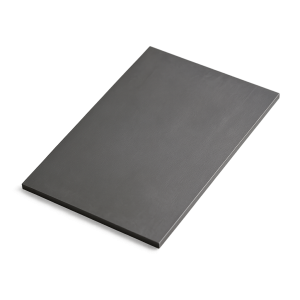
铅板(Pb Plate)是一种由高纯铅(Purity ≥ 99.9%)制成的高密度金属板材,具有优异的防辐射性能、耐腐蚀性和延展性
由于其对γ射线和X射线具有极强的吸收能力,铅板广泛用于辐射防护、医疗设备、实验室屏蔽、工业探伤、化工防腐与电池制造等领域。
其柔软、易加工且稳定的物理化学特性,使其成为放射防护与防腐工程中不可替代的关键材料。


产品详情

苏州科跃材料科技有限公司生产的高纯铅板采用真空熔炼—热轧—精整压延工艺制备,板面平整光滑、密度均匀、组织致密。
产品符合 ASTM B749 / GB/T 1470 / ISO 9001 标准,可提供工业级与医用防护级版本。

典型规格:

  • 纯度等级:99.9%、99.99%、99.999%

  • 厚度范围:0.5 – 50 mm

  • 宽度范围:≤ 1000 mm

  • 长度范围:≤ 2000 mm(可定制)

  • 制造工艺:真空熔炼 + 热轧 + 冷压延 + 光整处理

  • 表面状态:灰银色 / 抛光光亮 / 无氧化层


性能特点

  • 卓越的防辐射性能:高密度结构有效吸收X射线与γ射线。

  • 优异的耐腐蚀性:耐酸、耐碱、耐湿气。

  • 良好延展性:易于剪切、折弯与焊接。

  • 高密度与稳定性:密度高达11.34 g/cm³,化学性质稳定。

  • 可焊接与可粘合性好:适合多种结构安装与屏蔽系统。


应用领域

  • 医疗防护:用于X射线房、CT室、核医学防护墙及隔断。

  • 工业探伤:用于γ射线检测与屏蔽装置。

  • 核能与科研:实验室放射性屏蔽层与容器。

  • 化工防腐:用于酸槽内衬、吸收塔及管路防腐层。

  • 电池制造:用于铅酸蓄电池极板与电解装置。


技术参数

参数 典型值 / 范围 说明
纯度 99.9–99.999% 高纯度防护材料
密度 11.34 g/cm³ 高密度金属结构
熔点 327.5 °C 加工温度低
抗拉强度 12–17 MPa 柔软延展性好
延伸率 40–50% 易于冷加工
硬度 HB 5–10 软质金属
热导率 35 W/m·K 稳定导热性能
电导率 4.8 × 10⁶ S/m 一般导电性能
辐射吸收率 >95%(对X射线) 医疗级防护性能

常见问题(FAQ)

问题 答案
铅板能防辐射吗? 是的,对X射线和γ射线防护效果极佳。
是否有毒? 固态铅稳定,不会挥发;使用时应避免长期接触粉尘。
是否适合化工环境? 可用于酸性、碱性及湿气环境防腐。
是否可定制尺寸? 支持定制厚度、尺寸与切割。
是否可焊接? 可进行气焊、钎焊或机械连接。
是否符合环保要求? 提供RoHS、REACH与COC文件。
是否附检测报告? 附化学成分、密度与放射屏蔽检测报告。
是否适合科研用途? 是的,适用于屏蔽实验与材料研究。

包装与交付

所有铅板出厂前均经过密度与纯度检测,并进行表面防氧化处理。
产品采用防潮、防震、防腐包装,外层以出口级木箱固定。
提供 COC、RoHS/REACH、检测报告 等文件,可全球运输。

其他信息

首字母

Q

评价

目前还没有评价

成为第一个“铅板(Pb)” 的评价者

您的邮箱地址不会被公开。 必填项已用 * 标注

常见问题

Sputtering targets are materials used in thin-film deposition processes to create coatings on substrates. They are used in industries like semiconductors, optics, photovoltaics, and electronics.

Evaporation materials are used in Physical Vapor Deposition (PVD) processes, where materials are heated and evaporated to form a thin film on a substrate. These are critical for applications in optics, wear protection, and decorative coatings.

Boat crucibles are used as containers for evaporation materials during PVD processes. They help to uniformly evaporate materials onto the substrate for thin film formation.

Sputtering uses energetic particles to eject material from a target, while evaporation involves heating a material until it vaporizes and deposits on a substrate. Both are common methods in Physical Vapor Deposition (PVD) for creating thin films.

Consider the material composition, purity, target size, and application-specific requirements such as the thickness and uniformity of the film.

Yes, we offer customized sputtering targets, evaporation materials, and crucibles to meet specific customer requirements for size, material composition, and purity.

Yes, we can assist in selecting the most suitable material based on your application, whether it’s for optical coatings, semiconductor fabrication, or decorative finishes.

Yes, we offer both bulk and small quantities of sputtering targets, evaporation materials, and spherical powders to support research, prototyping, and development projects.