钽管(Ta)

描述

钽管(Ta Tube)

产品简介

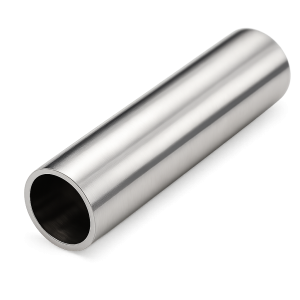
钽管(Ta Tube)是一种由高纯钽(Purity ≥ 99.9%)制成的高性能难熔金属管材,具有极高的熔点(3017°C)、优异的耐腐蚀性能和出色的延展性。钽在空气中会形成一层稳定的氧化膜(Ta₂O₅),使其在强酸、强碱和高温环境中依然保持化学惰性。
凭借高温强度、低蒸气压、良好导电性与高纯度结构,高纯钽管被广泛应用于真空设备、电子器件、半导体工艺及化学反应装置中。

产品详情

苏州科跃材料科技有限公司提供的高纯钽管采用**电子束熔炼(EBM)或真空电弧熔炼(VAR)**工艺制备,结构致密、纯度高、表面光洁。产品符合 ASTM B521、R05200 与 R05400 标准。

典型规格:

  • 纯度等级:99.9%、99.95%、99.99%

  • 外径范围:3 – 100 mm

  • 壁厚范围:0.3 – 6 mm

  • 长度:≤2000 mm(可定制)

  • 制造工艺:EBM / VAR 熔炼 → 挤压 → 冷拉 → 真空退火 → 精抛光

  • 表面状态:亮银灰色 / 抛光 / 去氧化膜 / 亚光

高纯钽管表面光滑、气体释放率低,可在高温真空及强腐蚀环境下长期使用。

应用领域

钽管因其高纯度与化学稳定性,在多个高端领域得到广泛应用:

  • 真空系统与电子设备:用于真空腔体、电子枪、蒸发源及导管结构。

  • 化工设备:用于强酸反应釜、热交换器与腐蚀性介质输送系统。

  • 半导体与光学镀膜:PVD、CVD系统的高纯导管与支撑组件。

  • 高温实验与冶金设备:用于保护管、加热腔与高温反应部件。

  • 医疗与航空领域:在惰性气氛中用于精密构件与高温连接系统。

技术参数

参数 典型值 / 范围 说明
纯度 99.9% – 99.99% 高纯度保证化学与热稳定性
密度 16.65 g/cm³ 结构致密,抗氧化性强
熔点 3017 °C 极高耐热性
抗拉强度 ≥500 MPa 强度高、塑性优良
热导率 57 W/m·K 良好导热性能
电导率 7.4 × 10⁶ S/m 稳定导电性能
工艺 EBM / VAR 熔炼 + 抛光 确保高纯与表面光洁度

常见问题(FAQ)

问题 答案
钽管是否能耐酸腐蚀? 是的,对几乎所有酸性介质均具优异耐蚀性,除氢氟酸外。
是否适合真空环境? 非常适合,钽的蒸气压极低,真空稳定性出色。
是否具磁性? 无磁性,适合磁场敏感设备。
可否焊接? 可采用电子束焊、氩弧焊及真空钎焊。
是否可电抛光? 可提供镜面或电解抛光表面。
能否制作薄壁管? 可定制至最小壁厚0.3 mm。
是否提供检测报告? 每批产品附带纯度、密度与尺寸检测报告。
是否支持小批量? 可提供科研样品与批量生产。
是否能与铌或钨合金化? 可提供TaNb、TaW合金版本。
使用寿命如何? 在高温真空或惰性气氛中可长期稳定使用。

包装与交付

所有钽管均经真空退火与纯度检测。产品采用真空密封+防潮防震包装,并外加木箱保护。提供RoHS、REACH、COC及材料分析报告,确保出口运输安全。

结论

钽管(Ta Tube)凭借其高熔点、耐腐蚀与高纯度特性,是高温真空、电子、化工及科研系统中的理想结构材料。
如需了解更多技术参数或获取报价,请联系:sales@keyuematerials.com

其他信息

首字母

T

评价

目前还没有评价

成为第一个“钽管(Ta)” 的评价者

您的邮箱地址不会被公开。 必填项已用 * 标注

常见问题

Sputtering targets are materials used in thin-film deposition processes to create coatings on substrates. They are used in industries like semiconductors, optics, photovoltaics, and electronics.

Evaporation materials are used in Physical Vapor Deposition (PVD) processes, where materials are heated and evaporated to form a thin film on a substrate. These are critical for applications in optics, wear protection, and decorative coatings.

Boat crucibles are used as containers for evaporation materials during PVD processes. They help to uniformly evaporate materials onto the substrate for thin film formation.

Sputtering uses energetic particles to eject material from a target, while evaporation involves heating a material until it vaporizes and deposits on a substrate. Both are common methods in Physical Vapor Deposition (PVD) for creating thin films.

Consider the material composition, purity, target size, and application-specific requirements such as the thickness and uniformity of the film.

Yes, we offer customized sputtering targets, evaporation materials, and crucibles to meet specific customer requirements for size, material composition, and purity.

Yes, we can assist in selecting the most suitable material based on your application, whether it’s for optical coatings, semiconductor fabrication, or decorative finishes.

Yes, we offer both bulk and small quantities of sputtering targets, evaporation materials, and spherical powders to support research, prototyping, and development projects.