金属间化合物 (BN-TiB₂) 电子束坩埚

基本信息

项目 参数说明
产品名称 BN-TiB₂ 电子束蒸发坩埚
材料组成 氮化硼 (BN) + 二硼化钛 (TiB₂) 复合陶瓷
成型方式 热压烧结 / 等静压成型
纯度等级 BN ≥ 99.5%,TiB₂ ≥ 99%
工作温度 ≥ 1800 °C(真空) / ≥ 1600 °C(惰性气氛)
外观颜色 深灰色 / 黑灰色复合陶瓷
适用设备 各类电子束蒸发镀膜机(如 PVD E-beam 系统)

描述

产品简介

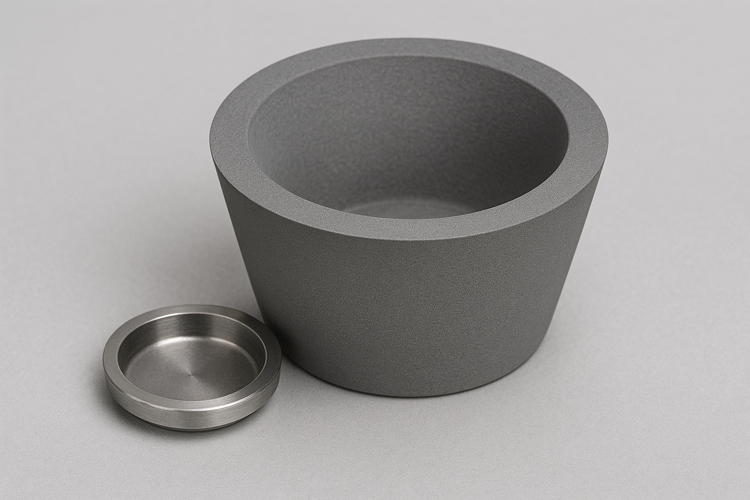
BN-TiB₂ 电子束坩埚 是由高纯氮化硼 (BN) 和二硼化钛 (TiB₂) 复合制备而成的高性能陶瓷坩埚,结合了 BN 的优异热稳定性和 TiB₂ 的电导率与强度。该坩埚特别适用于高真空条件下的电子束蒸发沉积工艺,能有效抑制材料溅射和污染,广泛应用于光学薄膜、半导体器件、太阳能电池、硬质涂层和其他精密镀膜工艺中。


BN-TiB₂ 坩埚的主要优势

  • 优异的抗热震性能:即使在高达 1800°C 的快速升降温环境中也能保持结构稳定

  • 高导电性:TiB₂ 成分赋予坩埚良好的电导率,便于电子束束斑均匀扩展,改善熔池形态

  • 抗熔蚀能力强:能承载高活性金属或化合物的蒸发(如铝、锆、钛、钽、氧化物等)

  • 化学惰性:BN 作为主要基体材料,具有极强的化学稳定性,不与绝大多数金属或气体反应

  • 寿命长,重复使用性高:陶瓷结构致密,耐蒸发辐照侵蚀,适合批量生产


典型规格(可定制)

外径 (mm) 高度 (mm) 壁厚 (mm) 适用 E-beam 电源 (kW) 型号参考
Ø50 30 4–5 3–5 BN-TiB2-50
Ø76 40 5–6 5–10 BN-TiB2-76
Ø100 50 6–8 10–15 BN-TiB2-100

※ 可根据客户图纸或镀膜腔体尺寸定制其他规格,如分区坩埚、多槽坩埚、内嵌冷却片等结构。


应用领域

  • ⚙️ 电子束蒸发沉积(E-beam evaporation)
    用于蒸发金属、氧化物、氟化物等材料进行真空镀膜

  • 🧪 半导体器件制造
    用于制造氧化物介电层、电极材料、功能薄膜

  • 🔬 光学镀膜 / 激光器件
    高折射率/低折射率材料交替沉积的精密应用

  • ☀️ 太阳能与光伏薄膜
    蒸发 Mo、Al、ZnO 等功能层材料,提升成膜均匀性与能效

  • 🛡 硬质涂层制备
    如 TiN、Al₂O₃ 等高温耐磨涂层材料的蒸发制备


包装与交付

  • 每件坩埚经超声波清洗,干燥真空密封

  • 使用定制泡沫托盘 + 双层硬纸箱,确保运输过程无破损

  • 可附带材质分析报告(XRD/EDS)及尺寸检验报告

  • 标准品现货供应,定制品交期通常 7–12 工作日


为什么选择苏州科跃材料的 BN-TiB₂ 坩埚?

  • ✔ 自有工厂,支持从粉体配比到烧结成型的全流程质量控制

  • ✔ 拥有 5 年以上出口经验,产品远销欧美与东南亚

  • ✔ 熟悉电子束蒸发工艺要求,配套技术指导

  • ✔ 支持与石墨/金属冷坩埚结构匹配设计

评价

目前还没有评价

成为第一个“金属间化合物 (BN-TiB₂) 电子束坩埚” 的评价者

您的邮箱地址不会被公开。 必填项已用 * 标注

常见问题

Sputtering targets are materials used in thin-film deposition processes to create coatings on substrates. They are used in industries like semiconductors, optics, photovoltaics, and electronics.

Evaporation materials are used in Physical Vapor Deposition (PVD) processes, where materials are heated and evaporated to form a thin film on a substrate. These are critical for applications in optics, wear protection, and decorative coatings.

Boat crucibles are used as containers for evaporation materials during PVD processes. They help to uniformly evaporate materials onto the substrate for thin film formation.

Sputtering uses energetic particles to eject material from a target, while evaporation involves heating a material until it vaporizes and deposits on a substrate. Both are common methods in Physical Vapor Deposition (PVD) for creating thin films.

Consider the material composition, purity, target size, and application-specific requirements such as the thickness and uniformity of the film.

Yes, we offer customized sputtering targets, evaporation materials, and crucibles to meet specific customer requirements for size, material composition, and purity.

Yes, we can assist in selecting the most suitable material based on your application, whether it’s for optical coatings, semiconductor fabrication, or decorative finishes.

Yes, we offer both bulk and small quantities of sputtering targets, evaporation materials, and spherical powders to support research, prototyping, and development projects.