硅晶圆

描述

精密硅晶圆供应商:苏州科跃材料科技有限公司

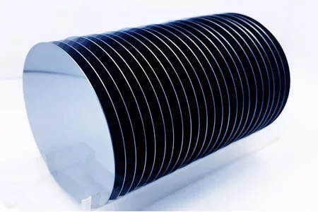
苏州科跃材料科技有限公司提供高品质硅(Si)晶圆,是现代半导体制造的核心材料。硅晶圆具有优异的电学性能、高热导率和良好的机械强度,被广泛应用于集成电路(IC)、微机电系统(MEMS)和功率电子器件中。

产品可提供多种直径、厚度及掺杂类型(N型或P型),适用于微处理器、光伏电池、传感器等多种应用领域。其超平整、低缺陷的表面有助于实现高质量的薄膜沉积和精密器件制造。

苏州科跃材料科技有限公司支持硅晶圆的定制服务,满足半导体科研、工业量产及先进技术开发的严格要求。


硅晶圆技术参数

  • 等级:Prime(主片)、Test(测试片)、Dummy(虚拟片)

  • 尺寸:10×10 mm、15×15 mm、20×15 mm、20×20 mm(支持定制)
    圆片直径:1″、2″、3″、4″、5″、6″、8″、12″

  • 厚度:0.3–0.5 mm、1.0 mm

  • 表面处理:单面抛光(SSP)或双面抛光(DSP)

  • 晶向:<100>、<110>、<111>

  • 晶向偏差:±0.5°

  • 倒角边角度:2°(可定制为1°)


硅晶圆物理性能

  • 材料:硅(Silicon)

  • 生长方式:区熔法(CZ)、磁控区熔法(MCZ)、浮区法(FZ)

  • 晶体结构:M3

  • 熔点:1420°C

  • 密度:2.4 g/cm³

  • 掺杂类型:无掺杂、硼(B)掺杂、磷(P)掺杂

  • 导电类型:P/N型、P型、N型

  • 电阻率:>1000 Ω·cm、10⁻³–40 Ω·cm、0.05–0.1 Ω·cm

  • 热膨胀系数:≤100/cm²


锑化镓晶圆(GaSb)

苏州科跃材料科技有限公司还供应锑化镓(GaSb)晶圆,广泛应用于红外器件、光电子器件以及半导体科研,性能卓越。我们可根据您的具体需求提供定制化解决方案,欢迎联系我们咨询。

评价

目前还没有评价

成为第一个“硅晶圆” 的评价者

您的邮箱地址不会被公开。 必填项已用 * 标注

常见问题

Sputtering targets are materials used in thin-film deposition processes to create coatings on substrates. They are used in industries like semiconductors, optics, photovoltaics, and electronics.

Evaporation materials are used in Physical Vapor Deposition (PVD) processes, where materials are heated and evaporated to form a thin film on a substrate. These are critical for applications in optics, wear protection, and decorative coatings.

Boat crucibles are used as containers for evaporation materials during PVD processes. They help to uniformly evaporate materials onto the substrate for thin film formation.

Sputtering uses energetic particles to eject material from a target, while evaporation involves heating a material until it vaporizes and deposits on a substrate. Both are common methods in Physical Vapor Deposition (PVD) for creating thin films.

Consider the material composition, purity, target size, and application-specific requirements such as the thickness and uniformity of the film.

Yes, we offer customized sputtering targets, evaporation materials, and crucibles to meet specific customer requirements for size, material composition, and purity.

Yes, we can assist in selecting the most suitable material based on your application, whether it’s for optical coatings, semiconductor fabrication, or decorative finishes.

Yes, we offer both bulk and small quantities of sputtering targets, evaporation materials, and spherical powders to support research, prototyping, and development projects.