砷化镓晶圆

砷化镓晶圆具备高电子迁移率、直接带隙和优异的高频性能,广泛应用于射频器件、激光器、红外探测器及高效太阳能电池。其出色的电学与光学特性使其成为高频通信与光电领域的关键材料。

描述

高频高速应用材料:苏州科跃材料科技有限公司提供砷化镓晶圆

苏州科跃材料科技有限公司专业供应高纯度砷化镓(GaAs)晶圆,具有直接带隙、高电子迁移率和优异的高频响应特性,广泛应用于射频(RF)器件、微波通信、红外探测、太阳能电池和光电子器件等领域。

砷化镓晶圆相比传统硅材料,在高速、高频及高功率应用中表现更佳,适用于制造HEMT、MESFET、pHEMT、LED、激光器、红外探测器以及高效率太阳能电池等器件。其晶格结构稳定,适合外延生长各类III-V族复合材料。

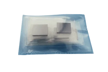
苏州科跃材料科技有限公司支持多种尺寸、晶向、掺杂方式的GaAs晶圆定制服务,确保优质晶体结构、极低缺陷密度与高表面光洁度,满足从科研到工业级应用的各类需求。


砷化镓晶圆规格参数

  • 尺寸:10×10 mm、15×15 mm、20×20 mm、25×25 mm、直径1″、2″、3″、4″、6″(可定制)

  • 厚度:350–650 μm(根据尺寸与工艺定制)

  • 晶向:<100>、<110>、<111>

  • 表面处理:单面抛光(SSP)、双面抛光(DSP)、带有外延生长表面(Epi-ready)

  • 掺杂类型:无掺杂、碳(C)、锌(Zn)(P型),硅(Si)、硒(Se)、锡(Sn)(N型)

  • 导电类型:N型、P型

  • 电阻率范围:0.001–10⁴ Ω·cm(可选)


砷化镓晶圆物理特性

  • 化学式:GaAs

  • 晶体结构:锌矿结构(Zinc Blende)

  • 晶格常数:a = 5.653 Å

  • 禁带宽度:1.42 eV(300 K,直接带隙)

  • 电子迁移率:~8,500 cm²/V·s(300 K)

  • 热导率:46 W/m·K

  • 熔点:1238°C

  • 密度:5.32 g/cm³

  • 折射率:~3.3(@λ=1 μm)

评价

目前还没有评价

成为第一个“砷化镓晶圆” 的评价者

您的邮箱地址不会被公开。 必填项已用 * 标注

常见问题

Sputtering targets are materials used in thin-film deposition processes to create coatings on substrates. They are used in industries like semiconductors, optics, photovoltaics, and electronics.

Evaporation materials are used in Physical Vapor Deposition (PVD) processes, where materials are heated and evaporated to form a thin film on a substrate. These are critical for applications in optics, wear protection, and decorative coatings.

Boat crucibles are used as containers for evaporation materials during PVD processes. They help to uniformly evaporate materials onto the substrate for thin film formation.

Sputtering uses energetic particles to eject material from a target, while evaporation involves heating a material until it vaporizes and deposits on a substrate. Both are common methods in Physical Vapor Deposition (PVD) for creating thin films.

Consider the material composition, purity, target size, and application-specific requirements such as the thickness and uniformity of the film.

Yes, we offer customized sputtering targets, evaporation materials, and crucibles to meet specific customer requirements for size, material composition, and purity.

Yes, we can assist in selecting the most suitable material based on your application, whether it’s for optical coatings, semiconductor fabrication, or decorative finishes.

Yes, we offer both bulk and small quantities of sputtering targets, evaporation materials, and spherical powders to support research, prototyping, and development projects.