钼板(Mo)

钼板(Mo Plate)以其高熔点、高强度、良好导热与真空稳定性,被广泛用于电子、半导体、光伏与真空设备中,是高温应用与精密制造的重要材料。

📩 联系邮箱: sales@keyuematerials.com

描述

钼板(Molybdenum Plate, Mo Plate)

产品简介

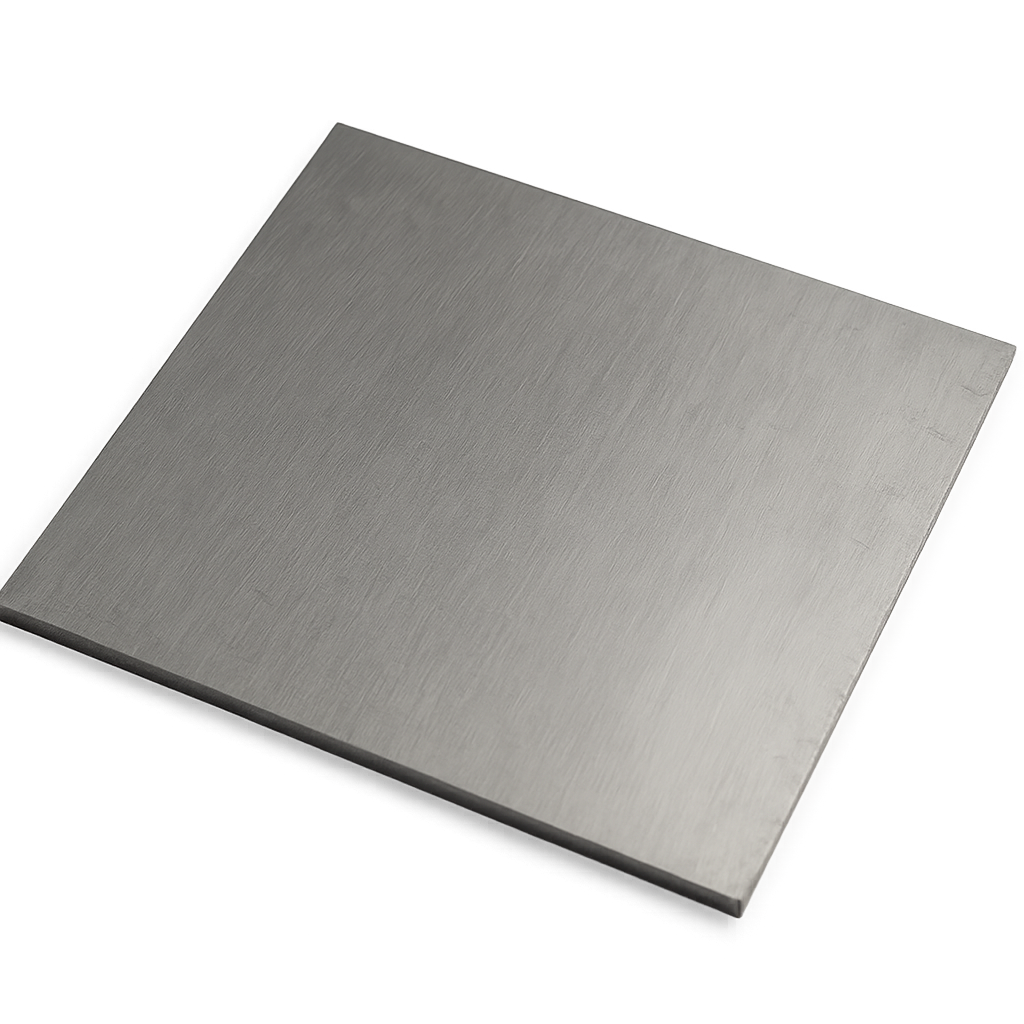
钼板(Mo Plate)是一种由高纯钼(Purity ≥ 99.9%–99.99%)制成的难熔金属板材,具有高熔点、高导热性、良好的机械强度和优异的耐腐蚀性
凭借这些特性,钼板在真空电子、半导体制造、冶金、玻璃熔融、电极和高温炉组件中广泛应用。


产品详情

苏州科跃材料科技有限公司生产的高纯钼板采用真空电子束熔炼(EBM)—热轧—真空退火—精抛光工艺制备,具有高纯度、低杂质、组织致密与优异平整度。
产品符合 ASTM B386 / GB/T 3876 / ISO 9001 标准,可提供科研级与工业级版本。

典型规格:

  • 纯度等级:99.9%、99.95%、99.99%

  • 厚度范围:0.2 – 25 mm

  • 尺寸范围:≤ 1000 × 1000 mm(可定制)

  • 制造工艺:真空熔炼 + 热轧 + 真空退火 + 抛光

  • 表面状态:银灰色 / 抛光光亮 / 无氧化层


性能特点

  • 超高熔点(2623 °C):适合极端高温环境。

  • 高导热与导电性:保证热稳定与电接触性能。

  • 抗热冲击与耐腐蚀:适用于真空与惰性气氛下工作。

  • 良好可加工性:可切割、焊接、折弯与抛光。

  • 高密度与低蒸气压:特别适合高真空系统使用。


应用领域

  • 电子与真空设备:用于电子管阴极、真空炉加热元件。

  • 半导体工业:用于溅射靶材、掩膜板、支撑片。

  • 玻璃与冶金工业:用于玻璃熔融电极与热屏。

  • 航空航天:用于高温结构件与火箭喷嘴衬层。

  • 能源与光伏行业:作为背电极、反射层或热场部件。


技术参数

参数 典型值 / 范围 说明
纯度 99.9–99.99% 高纯钼金属
密度 10.22 g/cm³ 致密结构
熔点 2623 °C 高温稳定性强
电导率 18.7 × 10⁶ S/m 导电性能优异
热导率 138 W/m·K 优良导热性
抗拉强度 400–600 MPa 高强度材料
延伸率 15–25% 良好延展性
硬度 HV 150–250 可退火调整
磁性 适用于真空设备
蒸气压 极低 适合高真空系统

常见问题(FAQ)

问题 答案
钼板是否具磁性? 无磁性。
是否可用于真空设备? 是,具有低蒸气压与高温稳定性。
是否可用于溅射或蒸发? 可用作溅射靶材或蒸发源。
是否耐酸碱腐蚀? 在酸碱中稳定,王水中会缓慢溶解。
是否可焊接? 可进行真空焊接或惰性气体保护焊。
是否提供检测报告? 附纯度及化学成分检测文件。
是否符合RoHS/REACH? 是,完全符合国际标准。
是否支持小批量? 提供科研样品及定制尺寸。
是否可抛光? 可提供镜面抛光表面。
交货周期? 常规规格2–3周内交付。

包装与交付

所有钼板出厂前均经真空退火与纯度检测
产品采用真空密封、防潮、防氧化包装,外层使用出口级木箱加固。
提供 COC、RoHS/REACH 文件与检测报告

其他信息

首字母

M

评价

目前还没有评价

成为第一个“钼板(Mo)” 的评价者

您的邮箱地址不会被公开。 必填项已用 * 标注

常见问题

Sputtering targets are materials used in thin-film deposition processes to create coatings on substrates. They are used in industries like semiconductors, optics, photovoltaics, and electronics.

Evaporation materials are used in Physical Vapor Deposition (PVD) processes, where materials are heated and evaporated to form a thin film on a substrate. These are critical for applications in optics, wear protection, and decorative coatings.

Boat crucibles are used as containers for evaporation materials during PVD processes. They help to uniformly evaporate materials onto the substrate for thin film formation.

Sputtering uses energetic particles to eject material from a target, while evaporation involves heating a material until it vaporizes and deposits on a substrate. Both are common methods in Physical Vapor Deposition (PVD) for creating thin films.

Consider the material composition, purity, target size, and application-specific requirements such as the thickness and uniformity of the film.

Yes, we offer customized sputtering targets, evaporation materials, and crucibles to meet specific customer requirements for size, material composition, and purity.

Yes, we can assist in selecting the most suitable material based on your application, whether it’s for optical coatings, semiconductor fabrication, or decorative finishes.

Yes, we offer both bulk and small quantities of sputtering targets, evaporation materials, and spherical powders to support research, prototyping, and development projects.