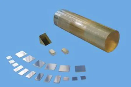
金红石衬底(TiO₂)
金红石衬底(TiO₂)是一种高折射率、低吸收损耗的优质光学单晶材料,因其优异的光学透明性、稳定的化学性质及良好的机械性能,被广泛应用于光学镀膜、光催化、非线性光学、铁电薄膜、光电子器件及表面科学研究等领域。其高介电常数和各向异性特性,使其在光调制器、波导、传感器以及高性能光学组件的制造中具有重要价值。
在外延生长方面,金红石衬底可与多种功能氧化物薄膜实现良好的晶格匹配,从而获得高质量的外延层结构。
物理性能
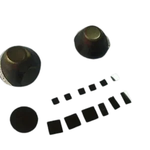
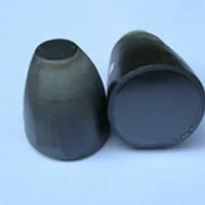
规格
包装
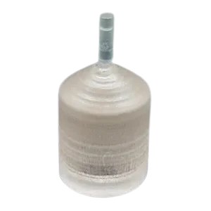
苏州科跃生产的金红石衬底在Class 1000级洁净室内切割、抛光与清洗,并采用Class 100洁净袋或晶圆盒进行密封包装,确保在运输和储存过程中免受污染。
这种高标准的加工与包装方式,使金红石衬底能够满足高端光学与光电子器件制造的严苛要求。