碳化硅晶圆(SiC)

描述

苏州科跃 碳化硅(SiC)晶圆:助力高科技未来

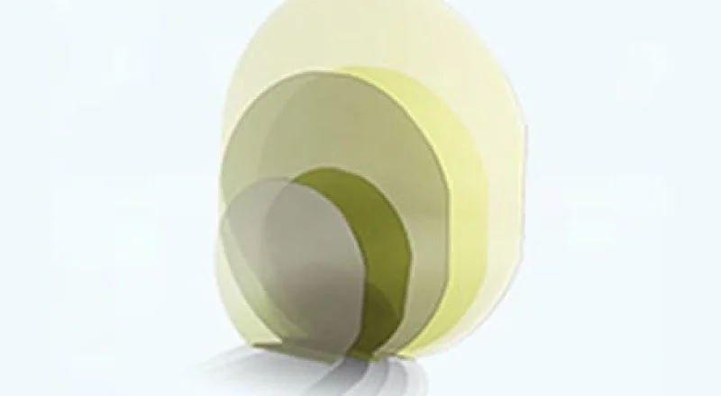
苏州科跃在碳化硅(SiC)晶圆生产领域处于行业领先地位,凭借卓越的品质与持续创新,为高科技产业提供可靠支持。结合丰富的制造经验与先进的生产技术,我们能够为客户定制满足现代应用需求的 SiC 晶圆解决方案。

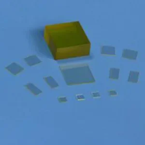
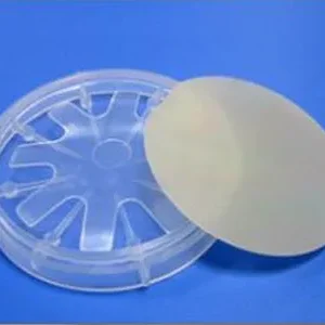
在苏州科跃,我们注重定制化与精密制造,确保每片晶圆都能为您的特定应用提供理想性能,助推先进技术的未来发展。

碳化硅晶圆规格

规格 参数
尺寸 10 × 3 mm、10 × 5 mm、10 × 10 mm、15 × 15 mm、20 × 15 mm、20 × 20 mm、直径 15 mm、直径 20 mm、直径 1″、直径 2″、直径 4″、直径 6″
厚度 0.35 mm
晶向 <0001>
抛光 单面抛光 (SSP) 或双面抛光 (DSP)
定向精度 ±0.5°
边缘倒角 2°(可选 1°)
晶体角度 可根据需求提供特殊尺寸与晶向
表面粗糙度 (Ra) ≤ 5 Å(5 μm × 5 μm)

碳化硅晶圆物理性能

性能参数 数值
材料 SiC
生长方法 MOCVD
晶体结构 M6
晶格常数 (Å) a = 3.08, c = 15.08
晶向 <0001> 3.5º
密度 (g/cm³) 3.21
莫氏硬度 9.2
熔点 1900°C
热传导率(@300K) 5 W/cm·K
介电常数 ε(11) = ε(22) = 9.66,ε(33) = 10.33

选择苏州科跃碳化硅晶圆,为您的下一代应用提供卓越性能、可靠性与精密度,满足先进半导体技术的未来发展需求。

评价

目前还没有评价

成为第一个“碳化硅晶圆(SiC)” 的评价者

您的邮箱地址不会被公开。 必填项已用 * 标注

常见问题

Sputtering targets are materials used in thin-film deposition processes to create coatings on substrates. They are used in industries like semiconductors, optics, photovoltaics, and electronics.

Evaporation materials are used in Physical Vapor Deposition (PVD) processes, where materials are heated and evaporated to form a thin film on a substrate. These are critical for applications in optics, wear protection, and decorative coatings.

Boat crucibles are used as containers for evaporation materials during PVD processes. They help to uniformly evaporate materials onto the substrate for thin film formation.

Sputtering uses energetic particles to eject material from a target, while evaporation involves heating a material until it vaporizes and deposits on a substrate. Both are common methods in Physical Vapor Deposition (PVD) for creating thin films.

Consider the material composition, purity, target size, and application-specific requirements such as the thickness and uniformity of the film.

Yes, we offer customized sputtering targets, evaporation materials, and crucibles to meet specific customer requirements for size, material composition, and purity.

Yes, we can assist in selecting the most suitable material based on your application, whether it’s for optical coatings, semiconductor fabrication, or decorative finishes.

Yes, we offer both bulk and small quantities of sputtering targets, evaporation materials, and spherical powders to support research, prototyping, and development projects.