多晶硅晶圆

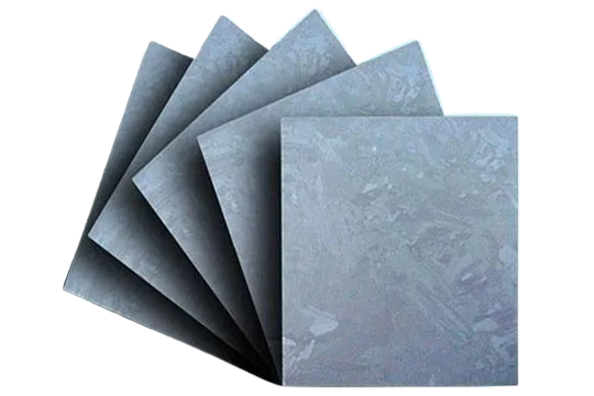
多晶硅晶圆由多个晶粒构成,具备良好的热稳定性和成本优势,广泛应用于太阳能电池、MEMS器件、光伏组件及中低端半导体工艺中,适合高性价比大规模制造需求。

描述

多晶硅晶圆(Polysilicon / Multicrystalline Wafer)

多晶硅晶圆是光伏电池制造中的关键材料,在多个行业中发挥着重要作用。这类晶圆广泛应用于光伏发电系统、通信、交通、边远地区住宅供电等场景,并在太阳能照明、草坪发电、屋顶太阳能系统等新兴领域中快速拓展。

苏州科跃材料科技有限公司生产的多晶硅晶圆具有优异的表面质量与高转换效率,可确保各种应用场景中的性能稳定性与可靠性。


多晶硅晶圆技术规格

参数项目 技术指标
材料 多晶硅(Polysilicon / Multicrystalline)
元素符号 Si
加工方式 金刚线切割(Diamond wire cutting)
导电类型/掺杂元素 P型或N型(如硼或镓)
边长尺寸 156.75–157.25 mm
厚度 200 ± 20 μm
转换效率 >18.8%

技术参数与材料性能

项目 数值及条件 测试方法/说明
晶体生长方式 DSS(定向凝固)
掺杂类型 P型:硼或镓掺杂 导电类型测试仪
电阻率(Ω·cm) 0.8~3.5 非接触式测试
晶体块载流子寿命(μs) ≥4 μs Semilab WT-2000D
表面反射率(纹理化) 17.5% ± 2.5% 标准扩散 +积分球 + 反射率仪
氧浓度(atoms/cm³) ≤5.0E17(10ppma) FTIR(ASTM F1188)
碳浓度(atoms/cm³) ≤5.0E17(10ppma) FTIR(ASTM F1391)

晶圆几何尺寸及结构特性

项目 技术指标 测量方法
边长 156.75 / 157.25 ± 0.25 mm 数显卡尺 / 晶圆检测系统
厚度 170–200 μm 晶圆检测系统
总厚度变化(TTV) ≤30 μm 晶圆检测系统
锯痕深度(Saw mark) ≤15 μm 晶圆检测系统
翘曲度(Warpage) ≤50 μm 晶圆检测系统
边缘垂直度 90° ± 0.3° CCD检测
倒角斜边(Hypotenuse) 0.45 – 2.00 mm 卡尺 / CCD
倒角直边(Cathetus) 0.31 – 1.42 mm
倒角角度 45° ± 10°

包装方式

每盒200片泡沫包装 → 每箱10盒 → 每托盘24箱,适用于出口运输和大批量出货,确保晶圆在运输过程中的安全与洁净。

评价

目前还没有评价

成为第一个“多晶硅晶圆” 的评价者

您的邮箱地址不会被公开。 必填项已用 * 标注

常见问题

Sputtering targets are materials used in thin-film deposition processes to create coatings on substrates. They are used in industries like semiconductors, optics, photovoltaics, and electronics.

Evaporation materials are used in Physical Vapor Deposition (PVD) processes, where materials are heated and evaporated to form a thin film on a substrate. These are critical for applications in optics, wear protection, and decorative coatings.

Boat crucibles are used as containers for evaporation materials during PVD processes. They help to uniformly evaporate materials onto the substrate for thin film formation.

Sputtering uses energetic particles to eject material from a target, while evaporation involves heating a material until it vaporizes and deposits on a substrate. Both are common methods in Physical Vapor Deposition (PVD) for creating thin films.

Consider the material composition, purity, target size, and application-specific requirements such as the thickness and uniformity of the film.

Yes, we offer customized sputtering targets, evaporation materials, and crucibles to meet specific customer requirements for size, material composition, and purity.

Yes, we can assist in selecting the most suitable material based on your application, whether it’s for optical coatings, semiconductor fabrication, or decorative finishes.

Yes, we offer both bulk and small quantities of sputtering targets, evaporation materials, and spherical powders to support research, prototyping, and development projects.