锑化镓晶圆

锑化镓晶圆具有窄带隙、高折射率和良好的红外透过性能,是红外探测器、中红外激光器、热电器件及高性能光电器件的重要基底材料,广泛用于红外成像、光谱分析与国防技术领域。

描述

锑化镓晶圆(Gallium Antimonide Wafer, GaSb)

锑化镓(GaSb)是III-V族半导体材料中的关键成员,广泛应用于中波至长波红外探测器和焦平面阵列,具备高灵敏度、可靠性强、寿命长等优势。GaSb晶圆广泛用于红外激光器、探测器、传感器以及热光伏电池等高端领域。


锑化镓晶圆物理性能

项目 参数说明
材料 GaSb(锑化镓)
生长方法 LEC、VGF、VBG
晶格常数(Å) a = 6.094
晶体结构 M3
熔点 712°C
密度(g/cm³) 5.53 g/cm³
掺杂类型 无掺杂、碲(Te)掺杂、锌(Zn)掺杂
导电类型 P型、P型、N型(按掺杂对应)
载流子浓度(cm⁻³) (1–2)×10¹⁷、(5–100)×10¹⁷、(1–20)×10¹⁸
迁移率(cm²/V·s) 600–700、200–500、2000–350(与掺杂相关)
缺陷密度(EPD) <2000/cm²、<2000/cm²、≤2000/≤500/cm²

锑化镓晶圆技术规格

项目 参数范围
晶圆尺寸 10×10 mm、10×5 mm、2″、3″(可定制)
厚度 500 µm、600 µm、800 µm(公差 ±25 µm)
表面处理 单面抛光(SSP)或双面抛光(DSP)
晶向 <100>、<111>
晶向偏差 ±0.5°
主定位边长度 16±2 mm、22±2 mm、32.5±2 mm
次定位边长度 8±1 mm、11±1 mm、18±1 mm
总厚度变化(TTV) <10 µm、<20 µm
弯曲度(Bow) <10 µm、<20 µm
翘曲度(Warp) <15 µm、<20 µm

锑化镓晶圆包装方式

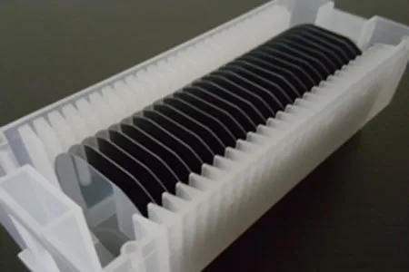
所有GaSb晶圆均在Class 1000洁净室内进行包装,采用Class 100洁净袋或专用晶圆盒密封包装,以确保材料洁净度并防止污染。

评价

目前还没有评价

成为第一个“锑化镓晶圆” 的评价者

您的邮箱地址不会被公开。 必填项已用 * 标注

常见问题

Sputtering targets are materials used in thin-film deposition processes to create coatings on substrates. They are used in industries like semiconductors, optics, photovoltaics, and electronics.

Evaporation materials are used in Physical Vapor Deposition (PVD) processes, where materials are heated and evaporated to form a thin film on a substrate. These are critical for applications in optics, wear protection, and decorative coatings.

Boat crucibles are used as containers for evaporation materials during PVD processes. They help to uniformly evaporate materials onto the substrate for thin film formation.

Sputtering uses energetic particles to eject material from a target, while evaporation involves heating a material until it vaporizes and deposits on a substrate. Both are common methods in Physical Vapor Deposition (PVD) for creating thin films.

Consider the material composition, purity, target size, and application-specific requirements such as the thickness and uniformity of the film.

Yes, we offer customized sputtering targets, evaporation materials, and crucibles to meet specific customer requirements for size, material composition, and purity.

Yes, we can assist in selecting the most suitable material based on your application, whether it’s for optical coatings, semiconductor fabrication, or decorative finishes.

Yes, we offer both bulk and small quantities of sputtering targets, evaporation materials, and spherical powders to support research, prototyping, and development projects.